The microcircuit chip is designed to be used in optical shaft encoders to implement diagnostics schemes and control Oof precision devices and mechanisms.
Catalog
products of microelectronics and microsystem technology
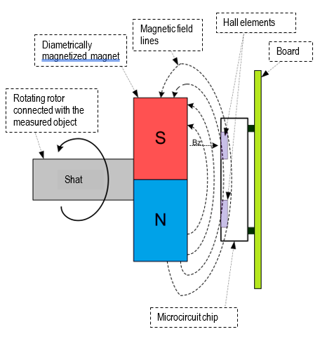
Transducers signals are maintained at the required level to ensure a steady operation in the range of distances between the microcircuit chip and rotating magnet.
Regulated signals arrive to Analog-Digital Converter to be converted. The calculated position code is represented as a set of standard digital and analog data transfer interfaces.
Communication Interfaces
Three-phase: UVW interface for brushless motors with two (four) pole rotor;Digital: as per SSI/SPI protocol ( slave type, SPI_MODE=0 for SPI mode);
PWM output;
Incremental: generates signals of 2 types:
- signals of incremental quarter-phaseinterface A/B/INDEX;
- signals of 'step+ direction' type STEP/DIR.
Analog: sine-cosine differential;
- Resolution: 12 bit;
- Output voltage range: 0.05…2.35 V (step 0.57);
- Maximal output current: 2 mA;
Benefits
- Single-chip placement (sensor and processing scheme);
- Possibility of of using external sensor;
- High precision;
- Nonsensitive to the constant component of magnetic field ±15mТ;
- Automatic adjustment to enhance sensor signals;
- Electrical calibration to simplify magnet alignment;
- Programmable hysteresis for reverse rotation;
- A broad choice of output interfaces;
- Low-profile housing.
| Range of measured angels: | 0…360°; |
| Programmable rotations counter: | 10 digits (up to 1024 rot.); |
| Rotational Speed1: | up to 60 thou. rpm; |
| Resolution: | 12 bit; (4096 reports per rotation); |
| Angular resolution: | 0.09° (5.3 min. ang.); |
| Conversion time: | 250 ns; |
| Conversion accuracy: | ± 0.35°; |
| Supply voltage2: | + 5 V ±10%; |
| Consumption current: | 30 mA; |
| Operating temperature range: | - 60… +125°C. |
| 1 - Maximal rotation speed can be limited by response speed of the output interface used. 2 - Supply voltage can be used +3.3 V. | |
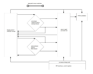
IC possesses embedded automated gain control (AGC) at variation of distance between magnet and IC.
To compensate for conversion error caused by inaccuracies of position sensor assembling IC has embedded unit of code position linearization.
IC settings are stored in external nonvolatile memory IC EEPROM with I2C interface (of 24LC01 type and similar ones).
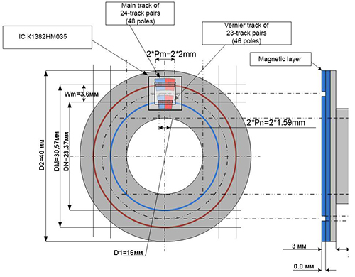
at creation of angular position sensors.
- Analogue output forms voltage proportional to current annular magnet position relative to sensor system;
- SSI/SPI interface is used for setting (programming) IC (in SPI mode) and issuing angular data (in SSI mode)
- OWI interface is used for setting (programming) IC, when access to SPI interface is disabled.
- Pulse width modulation (PWM) unit forms double-pusle sequence corresponding to angular code.
- Incremental interface forms incremental signals A/B/INDEX.
IC contains embedded temperature sensor unit designed to determine die temperature with resolution of 8 bit in temperature range: – 60 …+150 °C.
Applications
- Position sensors in inverted motor rotor;
- Robotics;
- Industrial position sensors;
- Position sensors for auto electronics.
| Maximum output voltage at outputs of PWM interface, V | UO.MAX not less than 0.9∙UСС |
| Minimum output voltage at outputs of PWM interface, V | UO.MIN less than 0.1∙UСС |
| Input voltage at low level at terminals of MISO, PO3, PO4, V | UOL less than 0.4 |
| Output voltage at high level at terminals of MISO, PO3, PO4, V | UOL not less than 2.4 |
| Current consumed by IC, mА (witout loading) | ICC less than 50 |
| Frequency of clock oscillator, MHz | fOSC not less than 50 |
| Maximum tracking frequency, kHz | fMAX.S not less than 2 |
| Maximum operating frequency of interface SPI, MHz: | fSPI not less than 4 |
| Maximum frequency of pulse width modulation interface, kHz | fPWM not less than 20 |
| Resolution of angular position readings on one pole pair, bit | RES not less than 12 |
| Maximum information capacity, natural units * | N 2(16)... 2(17) |
| Conversion error, deg. (with switched and tuned linearization) * | Err -0.2...+0.2 |
| Minimum magnetic field induction amplitude value, mT | BMIN less than 5 |
| Delay of signal propagation, microseconds | Td less than 50 |
| Operating temperature range, °С | T -40...+125 |
| * Measured at coded magnetic disk with 24 pole pairs. | |
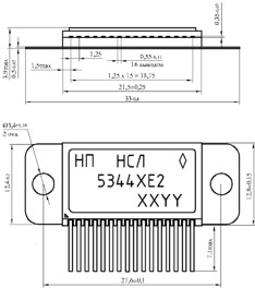
Applications
- Charging device;
- Battery management systems;
- Uninterruptible power supplies;
- Programmable power supplies;
- Tracking steering electric drives;
- Robotics.
Benefits
- High technical characteristics;
- Small dimensions;
- High accuracy;
- Noise immunity.
| Consumption current, mA: | ICC no more than 15 |
| Quiescent voltage of analog output, V: | UOUT0 from 2.425 to 2.575 |
| Temperature stability, %/С°: | αUOUT 0Q from -0.1 to 0.1 |
| Maximum analog output voltage, V: | U A OUT_MAX no less UCC - 0.55 |
| Minimum analog output voltage, V: | UAOUT_MIN no more than 0.55 |
| Analogue output current, mA: | Iout from 0.6 to 1.5 |
| Transfer coefficient of output characteristic, mV/A: | Ku no more than 66 |
| Low level voltage at the digital output, V : | UOL no more than 0.4 |
| High level voltage at the digital output, V : | UOH no less UCC - 0.4 |
| Speed characteristic, speed of the output voltage setting of the digital output, µs: | Tф no more than 1 |
| Generator frequency, MHz: | FOSC from 0.9 to 1.1 |
| PWM modulator frequency at the digital output, kHz: | FPWM from 110 to 140 |
| The operating cycle of the PWM modulator at the digital output ,%: | Q from 20 to 80 |
| Low level voltage at the nFAULT output, V : | UOLnFAULT no more than 0.4 |
| Threshold current of the nFAULT output operation, A: | ImeasnFAULT from ± 30 to ±60 |
| The value of the supply voltages of the analog blocks of the chip crystal, V: | UCC from 4.5 to 5.5 |
| The value of the supply voltages of the digital blocks of the chip crystal, V: | UDD from 2.97 to 3.6 3 |
| Built-in ROM programming voltage value, V: | UPP from 7.84 to 8.16 |
| Magnetic field measurement range, Gauss: | B from ± 600 to ± 670 |
| Measured current, A: | Imax no more than ±60 |
| Operating temperature range, С°: | T from -60 to 125 |
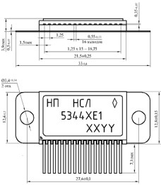
- Charging device;
- Battery management systems;
- Uninterruptible power supplies;
- Programmable power supplies;
- Tracking steering electric drives;
- Robotics.
Benefits
- High technical characteristics;
- Small dimensions;
- High accuracy;
- Noise immunity.
| Consumption current, mA: | ICC less than 15 |
| Quiescent voltage of the analog output, V: | UOUT0 from 2.425 to 2.575 |
| Temperature stability, %/С°: | αUOUT0Q from -0.1 to 0.1 |
| Maximum analog output voltage, V: | UAOUT_MAX more than UCC – 0.55 |
| Minimum analog output voltage, V: | UAOUT_MIN less than 0.55 |
| Analogue output current, mA: | Iout from 0.6 to 1.5 |
| Analogue output current, mA: | S from 3.0 to 3.25 |
| Linearity of the output characteristic, %: | L from -1.5 to 1.5 |
| The value of the supply voltages of the analog blocks of the chip crystal, V: | UCC from 4.5 to 5.5 |
| The value of the supply voltages of the digital blocks of the chip crystal, V: | UDD from 2.97 to 3.63 |
| Built-in ROM programming voltage value, V: | UPP from 7.84 to 8.16 |
| Magnetic field measurement range, Gauss: | B from ±600 to ±670 |
| Measured current, A: | Imax less than ±60 |
| Operating temperature range, С°: | T from -60 to 125 |
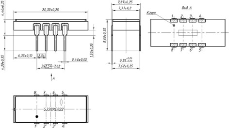
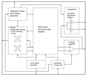
- Motor rotor position sensors;
- Movable nodes in robotics;
- Industrial position sensors;
- Position sensors for auto electronics;
- Replacement of potentiometers.
Benefits
- High accuracy;
- Compactness;
- Small consumption;
- Noise immunity.
| Consumption current, mА: | ICC less than 15 |
| Sensitivity to magnetic field induction, mTl: | S from 29.7 to 32.8 |
| Quiescent output voltage, V: | U0Q from 2.35 to 2.65 |
| Linearity of the output characteristic, %: | L from -1.5 to 1.5 |
| Temperature drift of quiescent voltage, %/С°: | α U0Q from -0.1 to 0.1 |
| Chip supply voltage, V: | UCC from 4.5 to 5.5 |
| Outflowing load current, mA: | IL_source more than 0.6 |
| Inflowing load current, mA: | IL_sink more than 1.0 |
| Operating temperature range, С°: | T from -60 to 125 |
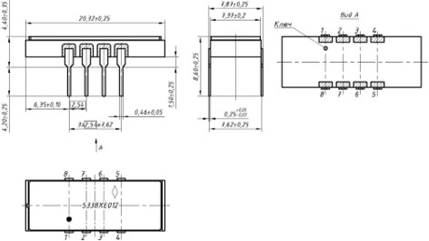
- Motor rotor position sensors;
- Movable nodes in robotics;
- Industrial position sensors;
- Position sensors for auto electronics;
- Replacement of potentiometers.
Benefits
- High accuracy;
- Compactness;
- Small consumption;
- Noise immunity.
| Consumption current, mA: | ICC less than 10 |
| Output 1 actuation induction, mT: | B ITP1 from 5 to 50 |
| Output 2 actuation induction , mT: | B ITP2 from 5 to 50 |
| Threshold setting accuracy, mTl: | δ BITP1 δ BITP2 less than 3.5 |
| Hysteresis of magnetic field induction, mTl: | BHYS1 Bgist2 more than 3 |
| Low level output voltage, V: | UOL1 UOL 2 less than 0.4 |
| Microcircuit supply voltage, V: | UCC from 4.5 to 5.5 |
| Load current, mA: | IL1 IL2 less than 20 |
| Operating temperature range, С°: | T from -60 to 125 |
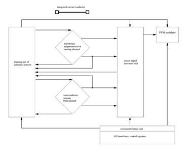
The microcircuit chip contains in-built system for correction of magnetic sensitive element's temperature dependence.

- Digital: SPI;
- Analog;
- PWM (Pulse Width Modulation );
- Logic output: open drain.
Benefits
- Noncontact current measurement;
- The presence of the internal transducer system;
- Possibility of connecting different types of external transducers;
- Coefficients and settings are stored in ЕEPROM non-volatile memory.
| Programmable current sensitivity: | (from 30 to 300 mV/A); |
| The differential signal voltage gain for inputs INP-INN: | 31.1÷50.82 un.; |
| Minimal detected current: | 10 mA; |
| Output supply current of the external sensitive element: | 1.45...2 mА; |
| Bandwidth: | 0÷50 kHz; |
| Resolution: | 12 bit; |
| Conversion accuracy: | ± 0.8 %; |
| Output voltage of the low-level comparator: | not more than +1 V; |
| Resolution of measuring the chip temperature: | not more than 2°С; |
| Open drain: | 30 mA; |
| Supply voltage: | + 5 V ± 10 %; |
| Consumption current: | not more than 25°mA; |
| Operating temperature range: | - 60…+125С. |
Specifications АЕНВ.431320.441.ТУ
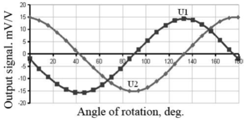
φ = 1/2(arctg(U1/U2))
- Domestic manufacturer;
- Delivery with acceptance “5”
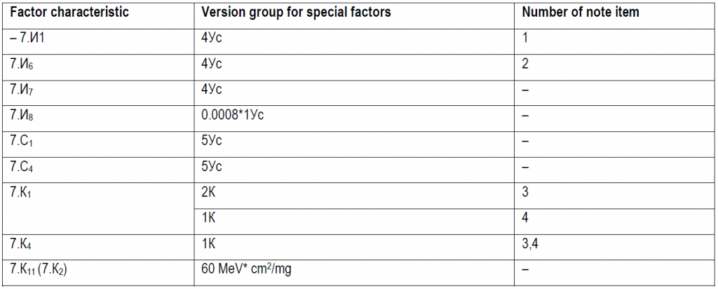
- By structural damage/defects.
- By catastrophic failures and by latch-up effect.
- In case of independent factors impact with characteristics 7.К1 and 7.К4.
- In case of combined factors impact with characteristics 7.К1 and 7.К4.
| Supply voltage | 5…10 V |
| Amplitude of output signal | Not less than 75 mV at U = 5 V |
| Resistance of one bridge | 2.5…3.5 kOhm |
| Bias voltage | ±1.5 mV/V |
| Hysteresis of output voltage, not more than | 0.1 % |
| Synchronism of output signals | 99…101 % |
| Range of measured angles | 0…180 º |
| Temperature coefficient of output voltage, less than; Less than | 0.35 %/°C at U = 5V; 0.13 %/°C at I = 2 mA |
| Temperature coefficient of bias voltage | ±2 (microV/V) /ºC |
| Temperature coefficient of one bridge resistance | 0.28 %/°C |
| Operating temperature range: | – 60…+125ºС. |
| Rotating planar magnetic field, not less than 25 kA/m | |
| IC possesses high resistance towards special factors impact | |
| IC is delivered in ceramic-and-metal package МК 5222.8-В, according to overall dimensions analog SO 8 (analog to SO 8 by dimensions) | |
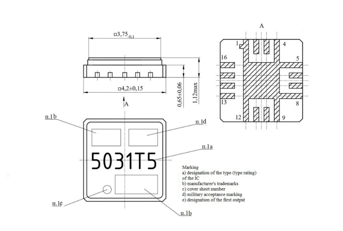
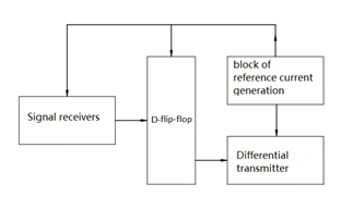
- Broadband testing and measurements;
- Serial data transmission;
- NRC to RZ conversion.
Benefits
- Supports high data rate;
- Differential and one-way operation;
- Low power consumption.
| Amplitude of differential output voltage, mV: | UOD from 350 to 1300 |
| Output voltage, V: | UO from UCC - 1.0 to UCC + 0.2 |
| Propagation delay time, ps: | tP less than 230 |
| Static current consumption, mA: | ICC less than 180 |
| Circuit core supply voltage, V: | UCC from 3.0 to 3.6 |
| Amplitude of the input differential voltage of the receiver, mV: | UID from 0.1 to 1.3 |
| Voltage at the differential receiver input, V : | UI from UCC - 1.5 to UCC |
| Control voltage of output signal amplitude, V : | UR from 0 to UCC |
| The frequency of the periodic signal of a rectangular shape with relative pulse duration of 2, at the microcircuit input, GHz: | FIN less than 13 |
| Data rate at the microcircuit input, Gbit / s : | DIN less than 13 |
| Operating temperature range, С °: | T from -60 to 85 |
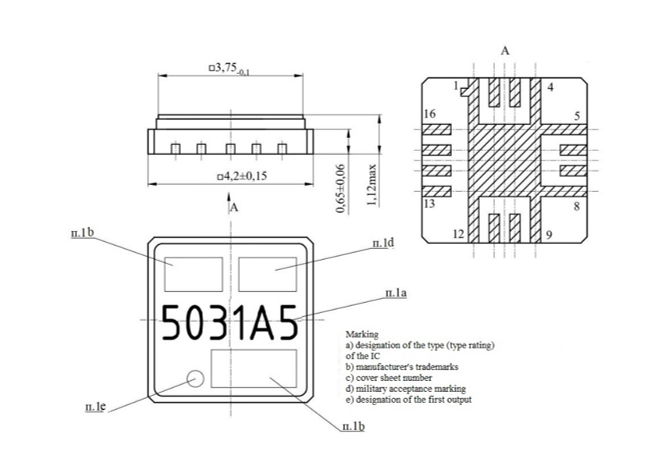

- Broadband testing and measurements;
- Serial data transmission;
- NRC to RZ conversion.
Benefits
- Supports high data rate;
- Differential and one-way operation;
- Low power consumption.
| Amplitude of differential output voltage, mV: | UOD from 350 to 1300 |
| Output voltage, V: | UO from UCC - 1.0 to UCC + 0.2 |
| Propagation delay time, ps: | tP less than 230 |
| Static current consumption, mA: | ICC less than 180 |
| Circuit core supply voltage, V: | UCC from 3.0 to 3.6 |
| Amplitude of the input differential voltage of the receiver, mV: | UID from 0.1 to 1.3 |
| Voltage at the differential receiver input, V: | UI from UCC - 1.5 to UCC |
| Control voltage of output signal amplitude, V: | UR from 0 to UCC |
| The frequency of the periodic signal of a rectangular shape with relative pulse duration of 2, at the microcircuit input, GHz: | FIN less than 13 |
| Data rate at the microcircuit input, Gbit/s: | DIN less than 13 |
| Operating temperature range, С°: | T from -60 to 85 |
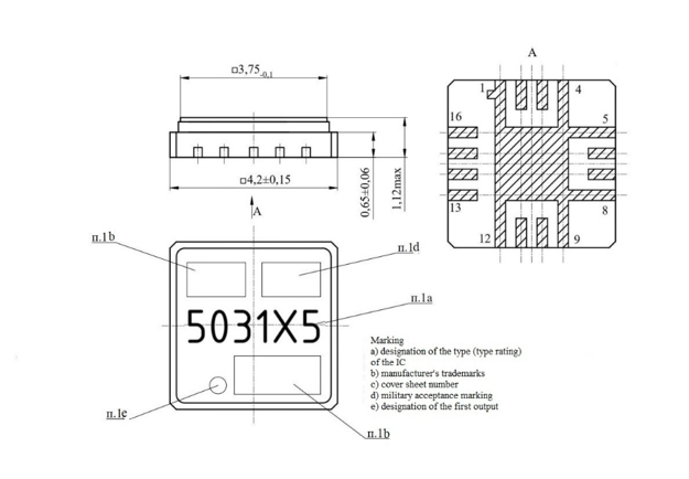
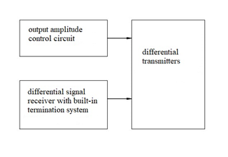
Applications:
- Broadband testing and measurements;
- Serial data transmission;
-
Clock buffering.
- Programmable differential;
- Differential and unilateral work;
- Low power consumption.
| Low level output voltage, V: | UOL no more than UCC - 1,65 |
| High level output voltage, V: | UOH more than UCC - 1,17 |
| Propagation delay time from CLK input to output, ps: | tPCLK less than 500 |
| Propagation delay time from SET, RESET input to output, ps: | tPSET less than 600 |
| Low level output leakage current on the inputs, uA: | ILL more than -50, less than 50 |
| High level output leakage current on the inputs, uA: | ILH more than -250, less than 250 |
| Static current consumption, mA: | ICC less than 150 |
| Circuit core supply voltage, V: | UCC more than 3,0, less than 3,6 |
| Low level of input voltage, V: | UIL more than UCC -1,80, less than UCC - 1,63 |
| High level of input voltage, V: | UIH more than UCC -1,20, less than UCC – 0,80 |
| Propagation delay time SET, RESET to the leading CLK edge, ps: | tRR more than 225 |
| Pulse width of SET, RESET signals, ps: | tPW more than 550 |
| Clock signal frequency at CLK input, GHz: | FCLK less than 3 |
| High level CLK signal pulse width, ps: | tCWH more than 166 |
| Low level CLK signal pulse width, ps: | tCWL more than 166 |
| Operating temperature range, С°: | Т from -60 to 85 |
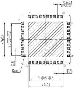
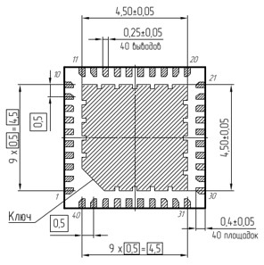
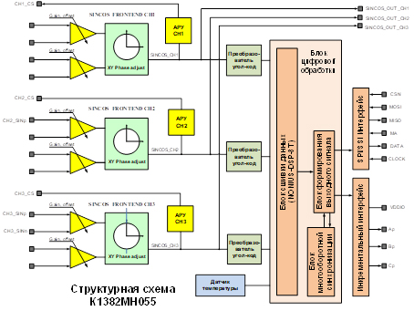
Filtered and demodulated signal arrives in CORR unit, which provides signal correction, including temperature compensation for bias voltage drift of input signals by embedded temperature sensor TEMP, independently for each channel, tuning amplification coefficients of channels, as well as phase shift compensation between channels.
Corrected signal arrives at tracking converter TRCV, which converts input signal into position code with resolution of 13 – 16 bits. Later position code is corrected depending on user settings in POSCV unit, number of revolutions is counted using MTURN counter, and combined position code arrives at interfaces circuits.
IC settings are saved in external nonvolatile memory EEPROM with I2C interface. Recommended memory type is 1644РС2Т.
- Single-chip placement (sensor and processing circuit);
- Possibility of using an external sensor;
- High accuracy;
- Insensitive to the constant component of the magnetic field ±15mT;
- Automatic gain control of sensor signals;
- Electrical calibration for easy magnet alignment;
- Programmable hysteresis for reverse rotation;
- Wide range of output interfaces;
- Small package;
- Domestic manufaturer;
- Possibility of military acceptance
Digital: via SSI/SPI protocol (type - slave, SPI_MODE=0 for SPI mode);
PWM output;
Incremental: generates 2 types of signals:
- A/B/INDEX incremental quadrature interface signals;
- STEP/DIR "step + direction" signals.
Analog: sine-cosine differential;
Analog lineral:
- Conversion bit depth: 12 bits;
- Output voltage level: 0.05…2.35 V (step 0.57);
- Maximum output current: 2 mA.
| Conversion resolution, bit: | Res 13 14 15 16 |
| Tracking rate (depending on resolution), not less than, Hz: | V Rate 244 122 61 30 |
| Transformation time ( depending on resolution), microseconds: | tc 8 10 12 15 |
| Error coordinates of changing code values, Е2: | number of not more than |
| Programmable reversible counter of revolutions: | Rev. up to 1024 |
| Load current of digital inputs, mА: | IIO not more than |
| Output voltage by analogue output, V: | Uo 0. 25.4.75 |
| Resolution of embedded temperature sensor, °С: | REST not more than 2 |
| Range of sine-cosine signal setting phase shift, deg: | DF0 – 30 ... +30 |
| Maximum operating frequency of interface SPI, MHz: | fspi not less than |
| Output synthesizer voltage amplitude (differential), V: | Uo.syn max not less than |
| Supply voltage, V | UCC 4.5 . 5.5 |
| Current consumption, mА: | ICC 15 |
| Output supply current of external sensor (at Rн = 1O0 Ohm), mA: | lo.sens 1.4 |
| Operating temperature range: | T –0 . +120 |


The microcircuit chip is designed to be used in optical shaft encoders to implement diagnostics schemes and control Oof precision devices and mechanisms.
Transducers signals are maintained at the required level to ensure a steady operation in the range of distances between the microcircuit chip and rotating magnet.
Regulated signals arrive to Analog-Digital Converter to be converted. The calculated position code is represented as a set of standard digital and analog data transfer interfaces.

Communication Interfaces
Three-phase: UVW interface for brushless motors with two (four) pole rotor;Digital: as per SSI/SPI protocol ( slave type, SPI_MODE=0 for SPI mode);
PWM output;
Incremental: generates signals of 2 types:
- signals of incremental quarter-phaseinterface A/B/INDEX;
- signals of 'step+ direction' type STEP/DIR.
Analog: sine-cosine differential;
- Resolution: 12 bit;
- Output voltage range: 0.05…2.35 V (step 0.57);
- Maximal output current: 2 mA;
Benefits
- Single-chip placement (sensor and processing scheme);
- Possibility of of using external sensor;
- High precision;
- Nonsensitive to the constant component of magnetic field ±15mТ;
- Automatic adjustment to enhance sensor signals;
- Electrical calibration to simplify magnet alignment;
- Programmable hysteresis for reverse rotation;
- A broad choice of output interfaces;
- Low-profile housing.
| Range of measured angels: | 0…360°; |
| Programmable rotations counter: | 10 digits (up to 1024 rot.); |
| Rotational Speed1: | up to 60 thou. rpm; |
| Resolution: | 12 bit; (4096 reports per rotation); |
| Angular resolution: | 0.09° (5.3 min. ang.); |
| Conversion time: | 250 ns; |
| Conversion accuracy: | ± 0.35°; |
| Supply voltage2: | + 5 V ±10%; |
| Consumption current: | 30 mA; |
| Operating temperature range: | - 60… +125°C. |
| 1 - Maximal rotation speed can be limited by response speed of the output interface used. 2 - Supply voltage can be used +3.3 V. | |

IC possesses embedded automated gain control (AGC) at variation of distance between magnet and IC.
To compensate for conversion error caused by inaccuracies of position sensor assembling IC has embedded unit of code position linearization.
IC settings are stored in external nonvolatile memory IC EEPROM with I2C interface (of 24LC01 type and similar ones).

at creation of angular position sensors.
- Analogue output forms voltage proportional to current annular magnet position relative to sensor system;
- SSI/SPI interface is used for setting (programming) IC (in SPI mode) and issuing angular data (in SSI mode)
- OWI interface is used for setting (programming) IC, when access to SPI interface is disabled.
- Pulse width modulation (PWM) unit forms double-pusle sequence corresponding to angular code.
- Incremental interface forms incremental signals A/B/INDEX.
IC contains embedded temperature sensor unit designed to determine die temperature with resolution of 8 bit in temperature range: – 60 …+150 °C.
Applications
- Position sensors in inverted motor rotor;
- Robotics;
- Industrial position sensors;
- Position sensors for auto electronics.
| Maximum output voltage at outputs of PWM interface, V | UO.MAX not less than 0.9∙UСС |
| Minimum output voltage at outputs of PWM interface, V | UO.MIN less than 0.1∙UСС |
| Input voltage at low level at terminals of MISO, PO3, PO4, V | UOL less than 0.4 |
| Output voltage at high level at terminals of MISO, PO3, PO4, V | UOL not less than 2.4 |
| Current consumed by IC, mА (witout loading) | ICC less than 50 |
| Frequency of clock oscillator, MHz | fOSC not less than 50 |
| Maximum tracking frequency, kHz | fMAX.S not less than 2 |
| Maximum operating frequency of interface SPI, MHz: | fSPI not less than 4 |
| Maximum frequency of pulse width modulation interface, kHz | fPWM not less than 20 |
| Resolution of angular position readings on one pole pair, bit | RES not less than 12 |
| Maximum information capacity, natural units * | N 2(16)... 2(17) |
| Conversion error, deg. (with switched and tuned linearization) * | Err -0.2...+0.2 |
| Minimum magnetic field induction amplitude value, mT | BMIN less than 5 |
| Delay of signal propagation, microseconds | Td less than 50 |
| Operating temperature range, °С | T -40...+125 |
| * Measured at coded magnetic disk with 24 pole pairs. | |
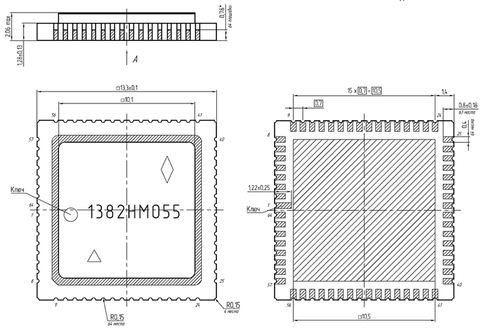
- master-channel,
- nonius sensor channel,
- segment-channel with 4…13 bit resolution (set in program), and further data crosslinking on obtaining output position code.
Microcircuit makes it possible to process master track signals with periods within 16 - 4096 range. Their number should be multiple of 2. If there are two code scales, channel 1 and channel are used.
Microcircuit has an inbuilt revolution counter with a programmable 24-digit counter module.
- Data on angle and revolutions number can be read out in SSI protocol in binary as well as in cyclic-binary code.
- Chip temperature code with 9 bit resolution can be read out via SPI/SSI interface.
- Analogue output allows bringing out analogue signals from analogue channel output.
- Setup parameters are stored using external EEPROM microcircuit with 12C interface. Recommended memory type is 1644PC2T, as well as 24C02.
Output interfaces
- Digital: (RS-422), SSI/SPI (transmitting angular data using SSI protocol, programming using SPI protocol).
- Incremental: (RS-422), forms signals of two types:
- signals of “step + direction” type (STEP/DIR).
- Analogue linear provides bringing-out of analogue signals from analogue channel output
Sphere of application
Systems of control of precise actuating mechanisms and drives in industrial equipment and robotics.
Competitive advantages
- Application of different types of external sensors (magnetoresistive, optical, Hall-effect sensors);
- Programmable conversion parameters;
- Automated adjustment of sensor signals parameters (amplitude, phase);
- Programmable counter of revolutions;
- Integtated temperature sensor;
- Programmable settings of output interfaces;
- Presentation of output interfaces through RS-422 driver;
- Small-sized package;
- Domestic manufacturer.
| Resolution of conversion | 4...13 bit |
| Bandwidth of analogue channel | at least 150 kHz |
| Resolution after nonius conversion | at least 21 bit |
| Time of conversion | not more than 250 ns |
| Programmable counter of revolutions | 24 bit |
| Frequency of SPI interface | 4 МHz |
| Supply voltage | +5V±10% |
| Current consumption | less than 50 mA |
| Load current of digital outputs | less than 4 mA |
| Operating temperature range | – 45 …+125°C |


Applications
- Charging device;
- Battery management systems;
- Uninterruptible power supplies;
- Programmable power supplies;
- Tracking steering electric drives;
- Robotics.
Benefits
- High technical characteristics;
- Small dimensions;
- High accuracy;
- Noise immunity.
| Consumption current, mA: | ICC no more than 15 |
| Quiescent voltage of analog output, V: | UOUT0 from 2.425 to 2.575 |
| Temperature stability, %/С°: | αUOUT 0Q from -0.1 to 0.1 |
| Maximum analog output voltage, V: | U A OUT_MAX no less UCC - 0.55 |
| Minimum analog output voltage, V: | UAOUT_MIN no more than 0.55 |
| Analogue output current, mA: | Iout from 0.6 to 1.5 |
| Transfer coefficient of output characteristic, mV/A: | Ku no more than 66 |
| Low level voltage at the digital output, V : | UOL no more than 0.4 |
| High level voltage at the digital output, V : | UOH no less UCC - 0.4 |
| Speed characteristic, speed of the output voltage setting of the digital output, µs: | Tф no more than 1 |
| Generator frequency, MHz: | FOSC from 0.9 to 1.1 |
| PWM modulator frequency at the digital output, kHz: | FPWM from 110 to 140 |
| The operating cycle of the PWM modulator at the digital output ,%: | Q from 20 to 80 |
| Low level voltage at the nFAULT output, V : | UOLnFAULT no more than 0.4 |
| Threshold current of the nFAULT output operation, A: | ImeasnFAULT from ± 30 to ±60 |
| The value of the supply voltages of the analog blocks of the chip crystal, V: | UCC from 4.5 to 5.5 |
| The value of the supply voltages of the digital blocks of the chip crystal, V: | UDD from 2.97 to 3.6 3 |
| Built-in ROM programming voltage value, V: | UPP from 7.84 to 8.16 |
| Magnetic field measurement range, Gauss: | B from ± 600 to ± 670 |
| Measured current, A: | Imax no more than ±60 |
| Operating temperature range, С°: | T from -60 to 125 |


- Charging device;
- Battery management systems;
- Uninterruptible power supplies;
- Programmable power supplies;
- Tracking steering electric drives;
- Robotics.
Benefits
- High technical characteristics;
- Small dimensions;
- High accuracy;
- Noise immunity.
| Consumption current, mA: | ICC less than 15 |
| Quiescent voltage of the analog output, V: | UOUT0 from 2.425 to 2.575 |
| Temperature stability, %/С°: | αUOUT0Q from -0.1 to 0.1 |
| Maximum analog output voltage, V: | UAOUT_MAX more than UCC – 0.55 |
| Minimum analog output voltage, V: | UAOUT_MIN less than 0.55 |
| Analogue output current, mA: | Iout from 0.6 to 1.5 |
| Analogue output current, mA: | S from 3.0 to 3.25 |
| Linearity of the output characteristic, %: | L from -1.5 to 1.5 |
| The value of the supply voltages of the analog blocks of the chip crystal, V: | UCC from 4.5 to 5.5 |
| The value of the supply voltages of the digital blocks of the chip crystal, V: | UDD from 2.97 to 3.63 |
| Built-in ROM programming voltage value, V: | UPP from 7.84 to 8.16 |
| Magnetic field measurement range, Gauss: | B from ±600 to ±670 |
| Measured current, A: | Imax less than ±60 |
| Operating temperature range, С°: | T from -60 to 125 |


- Motor rotor position sensors;
- Movable nodes in robotics;
- Industrial position sensors;
- Position sensors for auto electronics;
- Replacement of potentiometers.
Benefits
- High accuracy;
- Compactness;
- Small consumption;
- Noise immunity.
| Consumption current, mА: | ICC less than 15 |
| Sensitivity to magnetic field induction, mTl: | S from 29.7 to 32.8 |
| Quiescent output voltage, V: | U0Q from 2.35 to 2.65 |
| Linearity of the output characteristic, %: | L from -1.5 to 1.5 |
| Temperature drift of quiescent voltage, %/С°: | α U0Q from -0.1 to 0.1 |
| Chip supply voltage, V: | UCC from 4.5 to 5.5 |
| Outflowing load current, mA: | IL_source more than 0.6 |
| Inflowing load current, mA: | IL_sink more than 1.0 |
| Operating temperature range, С°: | T from -60 to 125 |


- Motor rotor position sensors;
- Movable nodes in robotics;
- Industrial position sensors;
- Position sensors for auto electronics;
- Replacement of potentiometers.
Benefits
- High accuracy;
- Compactness;
- Small consumption;
- Noise immunity.
| Consumption current, mA: | ICC less than 10 |
| Output 1 actuation induction, mT: | B ITP1 from 5 to 50 |
| Output 2 actuation induction , mT: | B ITP2 from 5 to 50 |
| Threshold setting accuracy, mTl: | δ BITP1 δ BITP2 less than 3.5 |
| Hysteresis of magnetic field induction, mTl: | BHYS1 Bgist2 more than 3 |
| Low level output voltage, V: | UOL1 UOL 2 less than 0.4 |
| Microcircuit supply voltage, V: | UCC from 4.5 to 5.5 |
| Load current, mA: | IL1 IL2 less than 20 |
| Operating temperature range, С°: | T from -60 to 125 |

Output interfaces
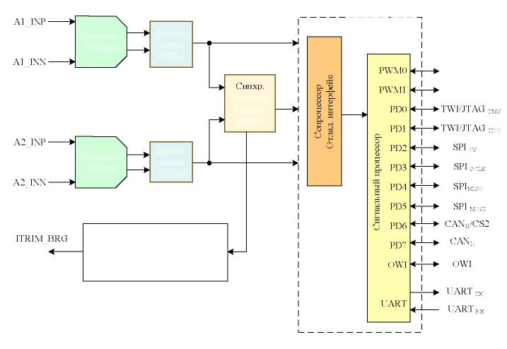
- CAN2.0b interface is full-function controller of CAN bus, contains 16 receive buffers, each of which is provided with its own message filter and eight transmitting buffers, built according to priority arbitrage.
- ОWI interface is designed for data exchange using single wire serial channel;
- Serial TWI interface;
- Serial SPI interface is designed for transmitting/receiving data in master and slave modes;
- PWM interface is multiphase special form signal generator, contains two channels and digitally measured number of digits (9, 10, 11, 12 bit);
- JTAG interface;
- Serial UART interface is designed to perform half-duplex asynchronous receiving and transmitting operations.
Special-purpose hardware as a low-consuming module of matching and processing signals received from precise temperature and pressure sensors. Provide high precision measurements, including initial part of operation range, long-term stability of calibration characteristics, fast response, wide range of output signals measurements, modern digital interfaces.
- Maximal ADC digits number, programmable conversion parameters;
- Wide range of programmable interfaces, enabling using it in different systems;
- Low energy consumption and wider, compared with analogue ones, range of operating temperature;
- Availability of embedded programmable current source enables one to use wider assortment of different types of external sensors;
- Domestic manufacturer.
| Number of analogue-to-digital converters | 2 |
| Digital-to-analog converter resolution | 18 bit |
| Maximal input differential voltage, V | not more than 0.4 V (at 2 times amplification) |
| •Digital-to-analog converter resolution | 12 bit |
| Number of signaling processor core digits | 16 |
| Volume of flesh memory | 8 k х 32 |
| Clock rate | 2…10 МHz |
| Supply voltage | 3.3 V ±0.33 |
| Current consumption | less than 1 mA |
| Operating temperature range | -60 …+125°C |
Transducer design responses to physical effect by increase of one of the capacitors (C1), while the other (C2), being in antiphase to it, decreases.
The microcircuit chip converts the change input containers into output voltage on analog output U.
Non-differential transducers can be used.
Temperature in-built transducer can be used to build temperature-independent systems. The microcircuit chip units contain programmable resistors and condensers for tuning parameters of the conversion path. Tuning is carried out by the microcircuit chip registers via SPI serial interface.
| The range of capacitances measured: | 1÷100 pF; |
| The range of output analog signal: | 0.3 ÷ (Ucc-0.3) V; |
| Output current: | max. +0.5 mA; |
| Low-level output voltage: | not more than 0.8 V |
| High-level output voltage: | not less than 2.8 V |
| Operating frequency of instrumentation amplifiers: | 19÷21 kHz; |
| Supply voltage (Ucc) | +3.3 V ±10%; |
| Consumption current: | not more than 3°mA; |
| Operating temperature range: | -60…+125°С. |


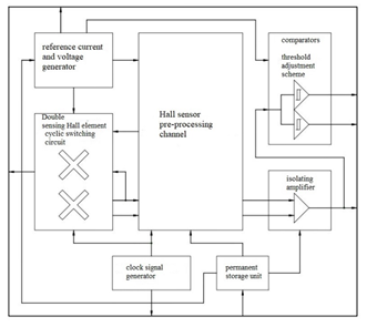
The microcircuit chip contains in-built system for correction of magnetic sensitive element's temperature dependence.

- Digital: SPI;
- Analog;
- PWM (Pulse Width Modulation );
- Logic output: open drain.
Benefits
- Noncontact current measurement;
- The presence of the internal transducer system;
- Possibility of connecting different types of external transducers;
- Coefficients and settings are stored in ЕEPROM non-volatile memory.


| Programmable current sensitivity: | (from 30 to 300 mV/A); |
| The differential signal voltage gain for inputs INP-INN: | 31.1÷50.82 un.; |
| Minimal detected current: | 10 mA; |
| Output supply current of the external sensitive element: | 1.45...2 mА; |
| Bandwidth: | 0÷50 kHz; |
| Resolution: | 12 bit; |
| Conversion accuracy: | ± 0.8 %; |
| Output voltage of the low-level comparator: | not more than +1 V; |
| Resolution of measuring the chip temperature: | not more than 2°С; |
| Open drain: | 30 mA; |
| Supply voltage: | + 5 V ± 10 %; |
| Consumption current: | not more than 25°mA; |
| Operating temperature range: | - 60…+125С. |
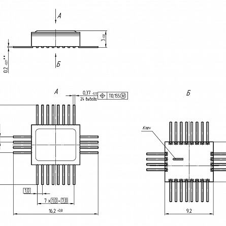
The microcircuit chip converts capacitance changes of differential bridge element into normalized value of electrical voltage for linear acceleration instrumentation.
Applications:
- Semiconductor capacitive acceleration transducer;
- Micro-electromechanical systems (MEMS), in.
Transducer design responses to physical effect by increase of one of the capacitors (C1), while the other (C2), being in antiphase to it, decreases.
The microcircuit chip converts the change input containers into output voltage on analog output U.
Non-differential transducers can be used.
Temperature in-built transducer can be used to build temperature-independent systems.
The microcircuit chip units contain programmable resistors and condensers for tuning parameters of the conversion path. Tuning is carried out by the microcircuit chip registers via SPI serial interface.
| The range of capacitances measured: | 1.5÷120 pF; |
| Maximal difference of the transducer capacitances converted by the microcircuit chip: | 50 pF; |
| Output analog signal range: | 0.5 ÷ 4.5 V; |
| Load current in digital outputs and comparator output: | not more than +2 mA; |
| Non-linearity of conversion characteristic: | not more than 5%; |
| Reference voltage: | 1.14÷1.26 V; |
| Operating rate of instrumentation amplifiers: | 110 kHz; |
| Supply voltage: | + 5 V ±10%; |
| Consumption current: | not more than 10°mA; |
| Operating temperature range: | -60…125°С. |

Specifications АЕНВ.431320.441.ТУ
φ = 1/2(arctg(U1/U2))

- Domestic manufacturer;
- Delivery with acceptance “5”

- By structural damage/defects.
- By catastrophic failures and by latch-up effect.
- In case of independent factors impact with characteristics 7.К1 and 7.К4.
- In case of combined factors impact with characteristics 7.К1 and 7.К4.
| Supply voltage | 5…10 V |
| Amplitude of output signal | Not less than 75 mV at U = 5 V |
| Resistance of one bridge | 2.5…3.5 kOhm |
| Bias voltage | ±1.5 mV/V |
| Hysteresis of output voltage, not more than | 0.1 % |
| Synchronism of output signals | 99…101 % |
| Range of measured angles | 0…180 º |
| Temperature coefficient of output voltage, less than; Less than | 0.35 %/°C at U = 5V; 0.13 %/°C at I = 2 mA |
| Temperature coefficient of bias voltage | ±2 (microV/V) /ºC |
| Temperature coefficient of one bridge resistance | 0.28 %/°C |
| Operating temperature range: | – 60…+125ºС. |
| Rotating planar magnetic field, not less than 25 kA/m | |
| IC possesses high resistance towards special factors impact | |
| IC is delivered in ceramic-and-metal package МК 5222.8-В, according to overall dimensions analog SO 8 (analog to SO 8 by dimensions) | |
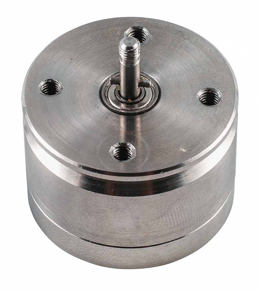
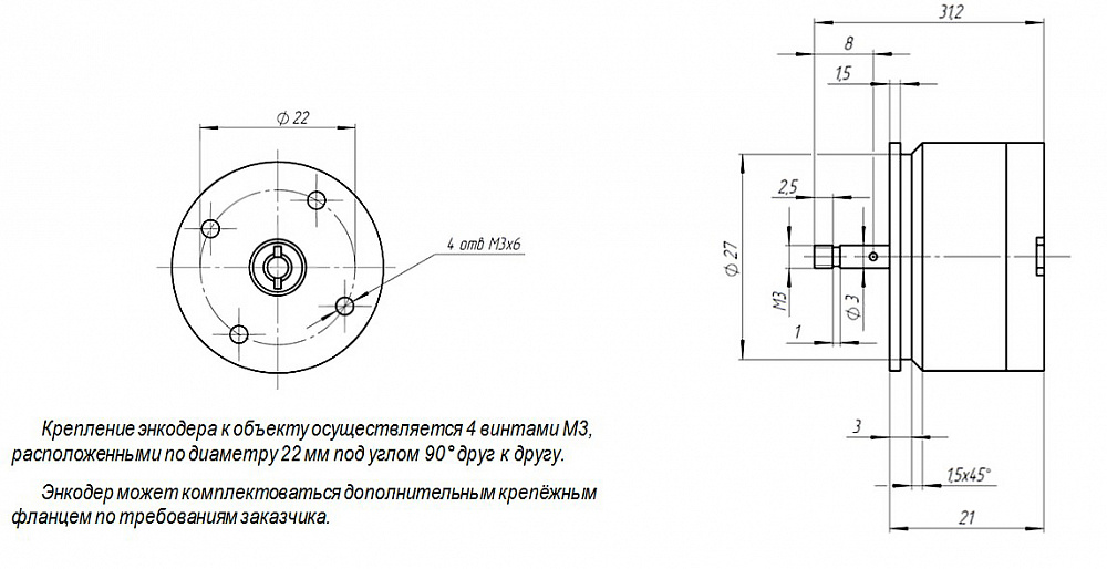
| Angular resolution: | 5,3 ang. min; |
| Steps per turn: | 4,096; |
| Measurement error: | not more than +0.35°; |
| Rotational speed1: | max. 20000 rpm; |
| Supply voltage: | +5 ±10% V; |
| Consumption current: | 50 mА; |
| Operating temperature range: | - 60…+125°С; |
| *rotation speed can be limited by response speed of the output interface used. | |
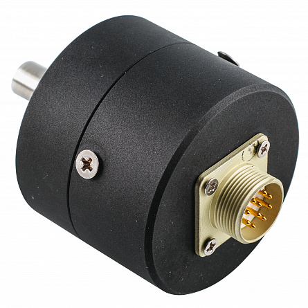
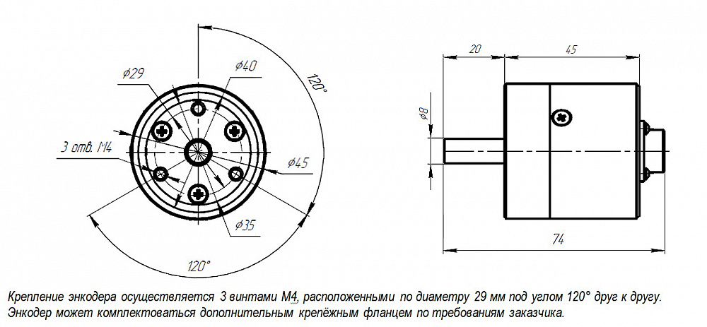
| Angular resolution: | 5,3 ang. min; |
| Steps per turn: | 4,096; |
| Measurement error: | not more than +5%; |
| Rotation speed1: | max.10000 rpm; |
| Supply voltage: | +7…30 V; |
| Consumption current: | not more than 30°mA; |
| Operating temperature range: | - 40…+85°С; |
| Weight: | 200 g |


- Broadband testing and measurements;
- Serial data transmission;
- NRC to RZ conversion.
Benefits
- Supports high data rate;
- Differential and one-way operation;
- Low power consumption.
| Amplitude of differential output voltage, mV: | UOD from 350 to 1300 |
| Output voltage, V: | UO from UCC - 1.0 to UCC + 0.2 |
| Propagation delay time, ps: | tP less than 230 |
| Static current consumption, mA: | ICC less than 180 |
| Circuit core supply voltage, V: | UCC from 3.0 to 3.6 |
| Amplitude of the input differential voltage of the receiver, mV: | UID from 0.1 to 1.3 |
| Voltage at the differential receiver input, V : | UI from UCC - 1.5 to UCC |
| Control voltage of output signal amplitude, V : | UR from 0 to UCC |
| The frequency of the periodic signal of a rectangular shape with relative pulse duration of 2, at the microcircuit input, GHz: | FIN less than 13 |
| Data rate at the microcircuit input, Gbit / s : | DIN less than 13 |
| Operating temperature range, С °: | T from -60 to 85 |


- Broadband testing and measurements;
- Serial data transmission;
- NRC to RZ conversion.
Benefits
- Supports high data rate;
- Differential and one-way operation;
- Low power consumption.
| Amplitude of differential output voltage, mV: | UOD from 350 to 1300 |
| Output voltage, V: | UO from UCC - 1.0 to UCC + 0.2 |
| Propagation delay time, ps: | tP less than 230 |
| Static current consumption, mA: | ICC less than 180 |
| Circuit core supply voltage, V: | UCC from 3.0 to 3.6 |
| Amplitude of the input differential voltage of the receiver, mV: | UID from 0.1 to 1.3 |
| Voltage at the differential receiver input, V: | UI from UCC - 1.5 to UCC |
| Control voltage of output signal amplitude, V: | UR from 0 to UCC |
| The frequency of the periodic signal of a rectangular shape with relative pulse duration of 2, at the microcircuit input, GHz: | FIN less than 13 |
| Data rate at the microcircuit input, Gbit/s: | DIN less than 13 |
| Operating temperature range, С°: | T from -60 to 85 |


Applications:
- Broadband testing and measurements;
- Serial data transmission;
-
Clock buffering.
- Programmable differential;
- Differential and unilateral work;
- Low power consumption.
| Low level output voltage, V: | UOL no more than UCC - 1,65 |
| High level output voltage, V: | UOH more than UCC - 1,17 |
| Propagation delay time from CLK input to output, ps: | tPCLK less than 500 |
| Propagation delay time from SET, RESET input to output, ps: | tPSET less than 600 |
| Low level output leakage current on the inputs, uA: | ILL more than -50, less than 50 |
| High level output leakage current on the inputs, uA: | ILH more than -250, less than 250 |
| Static current consumption, mA: | ICC less than 150 |
| Circuit core supply voltage, V: | UCC more than 3,0, less than 3,6 |
| Low level of input voltage, V: | UIL more than UCC -1,80, less than UCC - 1,63 |
| High level of input voltage, V: | UIH more than UCC -1,20, less than UCC – 0,80 |
| Propagation delay time SET, RESET to the leading CLK edge, ps: | tRR more than 225 |
| Pulse width of SET, RESET signals, ps: | tPW more than 550 |
| Clock signal frequency at CLK input, GHz: | FCLK less than 3 |
| High level CLK signal pulse width, ps: | tCWH more than 166 |
| Low level CLK signal pulse width, ps: | tCWL more than 166 |
| Operating temperature range, С°: | Т from -60 to 85 |


Applications
- Charging device;
- Battery management systems;
- Uninterruptible power supplies;
- Programmable power supplies;
- Tracking steering electric drives;
- Robotics.
Benefits
- High technical characteristics;
- Small dimensions;
- High accuracy;
- Noise immunity.
| Consumption current, mA: | ICC no more than 15 |
| Quiescent voltage of analog output, V: | UOUT0 from 2.425 to 2.575 |
| Temperature stability, %/С°: | αUOUT 0Q from -0.1 to 0.1 |
| Maximum analog output voltage, V: | U A OUT_MAX no less UCC - 0.55 |
| Minimum analog output voltage, V: | UAOUT_MIN no more than 0.55 |
| Analogue output current, mA: | Iout from 0.6 to 1.5 |
| Transfer coefficient of output characteristic, mV/A: | Ku no more than 66 |
| Low level voltage at the digital output, V : | UOL no more than 0.4 |
| High level voltage at the digital output, V : | UOH no less UCC - 0.4 |
| Speed characteristic, speed of the output voltage setting of the digital output, µs: | Tф no more than 1 |
| Generator frequency, MHz: | FOSC from 0.9 to 1.1 |
| PWM modulator frequency at the digital output, kHz: | FPWM from 110 to 140 |
| The operating cycle of the PWM modulator at the digital output ,%: | Q from 20 to 80 |
| Low level voltage at the nFAULT output, V : | UOLnFAULT no more than 0.4 |
| Threshold current of the nFAULT output operation, A: | ImeasnFAULT from ± 30 to ±60 |
| The value of the supply voltages of the analog blocks of the chip crystal, V: | UCC from 4.5 to 5.5 |
| The value of the supply voltages of the digital blocks of the chip crystal, V: | UDD from 2.97 to 3.6 3 |
| Built-in ROM programming voltage value, V: | UPP from 7.84 to 8.16 |
| Magnetic field measurement range, Gauss: | B from ± 600 to ± 670 |
| Measured current, A: | Imax no more than ±60 |
| Operating temperature range, С°: | T from -60 to 125 |


- Charging device;
- Battery management systems;
- Uninterruptible power supplies;
- Programmable power supplies;
- Tracking steering electric drives;
- Robotics.
Benefits
- High technical characteristics;
- Small dimensions;
- High accuracy;
- Noise immunity.
| Consumption current, mA: | ICC less than 15 |
| Quiescent voltage of the analog output, V: | UOUT0 from 2.425 to 2.575 |
| Temperature stability, %/С°: | αUOUT0Q from -0.1 to 0.1 |
| Maximum analog output voltage, V: | UAOUT_MAX more than UCC – 0.55 |
| Minimum analog output voltage, V: | UAOUT_MIN less than 0.55 |
| Analogue output current, mA: | Iout from 0.6 to 1.5 |
| Analogue output current, mA: | S from 3.0 to 3.25 |
| Linearity of the output characteristic, %: | L from -1.5 to 1.5 |
| The value of the supply voltages of the analog blocks of the chip crystal, V: | UCC from 4.5 to 5.5 |
| The value of the supply voltages of the digital blocks of the chip crystal, V: | UDD from 2.97 to 3.63 |
| Built-in ROM programming voltage value, V: | UPP from 7.84 to 8.16 |
| Magnetic field measurement range, Gauss: | B from ±600 to ±670 |
| Measured current, A: | Imax less than ±60 |
| Operating temperature range, С°: | T from -60 to 125 |


- Motor rotor position sensors;
- Movable nodes in robotics;
- Industrial position sensors;
- Position sensors for auto electronics;
- Replacement of potentiometers.
Benefits
- High accuracy;
- Compactness;
- Small consumption;
- Noise immunity.
| Consumption current, mА: | ICC less than 15 |
| Sensitivity to magnetic field induction, mTl: | S from 29.7 to 32.8 |
| Quiescent output voltage, V: | U0Q from 2.35 to 2.65 |
| Linearity of the output characteristic, %: | L from -1.5 to 1.5 |
| Temperature drift of quiescent voltage, %/С°: | α U0Q from -0.1 to 0.1 |
| Chip supply voltage, V: | UCC from 4.5 to 5.5 |
| Outflowing load current, mA: | IL_source more than 0.6 |
| Inflowing load current, mA: | IL_sink more than 1.0 |
| Operating temperature range, С°: | T from -60 to 125 |


- Motor rotor position sensors;
- Movable nodes in robotics;
- Industrial position sensors;
- Position sensors for auto electronics;
- Replacement of potentiometers.
Benefits
- High accuracy;
- Compactness;
- Small consumption;
- Noise immunity.
| Consumption current, mA: | ICC less than 10 |
| Output 1 actuation induction, mT: | B ITP1 from 5 to 50 |
| Output 2 actuation induction , mT: | B ITP2 from 5 to 50 |
| Threshold setting accuracy, mTl: | δ BITP1 δ BITP2 less than 3.5 |
| Hysteresis of magnetic field induction, mTl: | BHYS1 Bgist2 more than 3 |
| Low level output voltage, V: | UOL1 UOL 2 less than 0.4 |
| Microcircuit supply voltage, V: | UCC from 4.5 to 5.5 |
| Load current, mA: | IL1 IL2 less than 20 |
| Operating temperature range, С°: | T from -60 to 125 |

