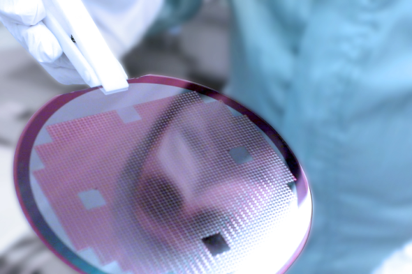
Full manufacturing cycle
The set of manufacturing routes implemented by ZNTC allows to carry out a full cycle of technological services in the field of creating microelectronic products and microsystem equipment, as well as to implement individual technological operations of ICs manufacturing (manufacturing of VLSI, MEMS, SoC).

Services
- MEMS magnetoresistive sensors and transducers
- MEMS angular velocity sensors (gyroscopes, accelerometers)
- Integral photonics elements
- Power electronics (GaN-HEMT, IGBT)
- Pin diodes, NMOS

Advantages
- Ability to reduce customer costs
- for the manufacturing of ICs and MPW
- -projects, technology development and fine
- tuning of some product parameters.
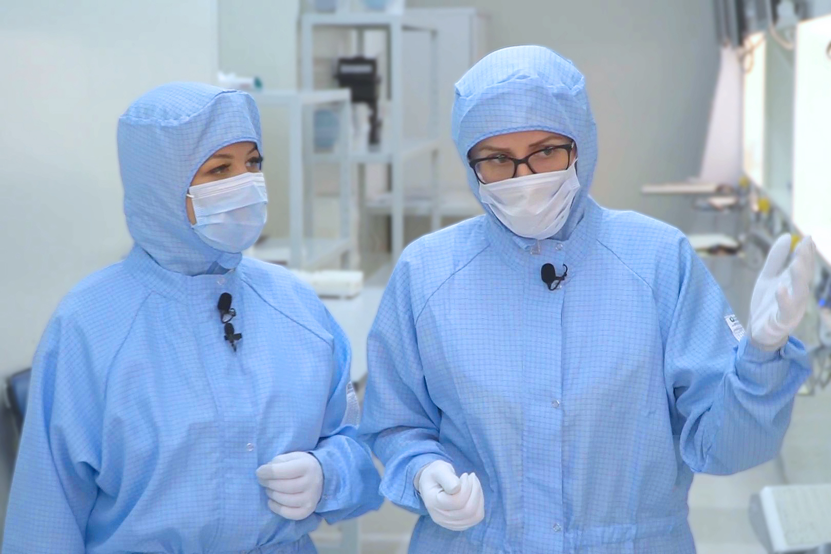
- Completely Russian-made production
- at all stages of product manufacturing,
- including design, photomasking and ICs
- manufacturing and testing.
We always take into account customer needs and are ready to work on new interesting projects to expand our production capabilities.
Get a commercial offer
Send your details and we will contact you
* Required fields