Zelenograd Nanotechnology Center will participate in the development of the domestic maskless lithograph
Research work on developing a maskless X-ray nanolithography tool with a wavelength of 13.5 nm based on a synchrotron and/or plasma source is carried out by scientists from the Center for Collective Usage "Microsystem Technology and Electronic Component Base" of MIET. If the research is successful, a unique equipment tool will appear in Russia to manufacture chips with a topological level of 28 nm or less.
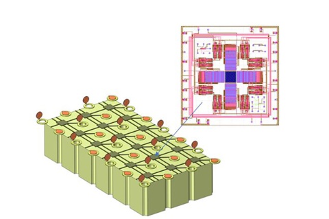
The research is aimed at the experimental verification of the main technological solutions in the field of maskless X-ray nanolithography. The first stage of the project involves the manufacture and experimental study of dynamic mask MEMS models in two design options: with X-ray transmittance control and with X-ray reflectance control. Based on the obtained results, the parameters of the key components will be developed: an X-ray source, an optical system (including a dynamic mask MEMS), a vacuum system, an alignment and positioning system.
Technology and equipment based on domestic synchrotrons, as well as on the basis of domestic plasma sources, will allow processing semiconductor wafers with design standards of 28 nm, 16 nm and less.
There are currently no domestic and world analogues of such equipment and the technology of maskless X-ray nanolithography.
The project team consists of about 50 MIET employees, including young candidates of sciences and postgraduates. MIET partners also work on the project: Mikron group and Zelenograd Nanotechnology Center - their production capabilities will be used to manufacture samples of the MEMS dynamic mask. The Institute of Physics of Microstructures of the Russian Academy of Sciences (Nizhny Novgorod) and JSC “NPP “ESTO” develop an optical vacuum system with mirror optics and elements of a positioning system.
